The semiconductor industry has reached a pivotal juncture where traditional monolithic chip design can no longer keep pace with the exponential demands of generative artificial intelligence. As silicon scaling slows, the focus of hardware innovation has shifted from making transistors smaller to making systems smarter. The most significant breakthrough in the last 12 months is the arrival of NVIDIA’s Blackwell architecture, a physical hardware marvel that moves the industry from “chips” to data center scale silicon.
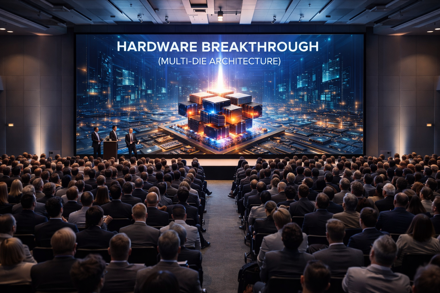
The Physical Breakthrough: Multi-Die Interconnects
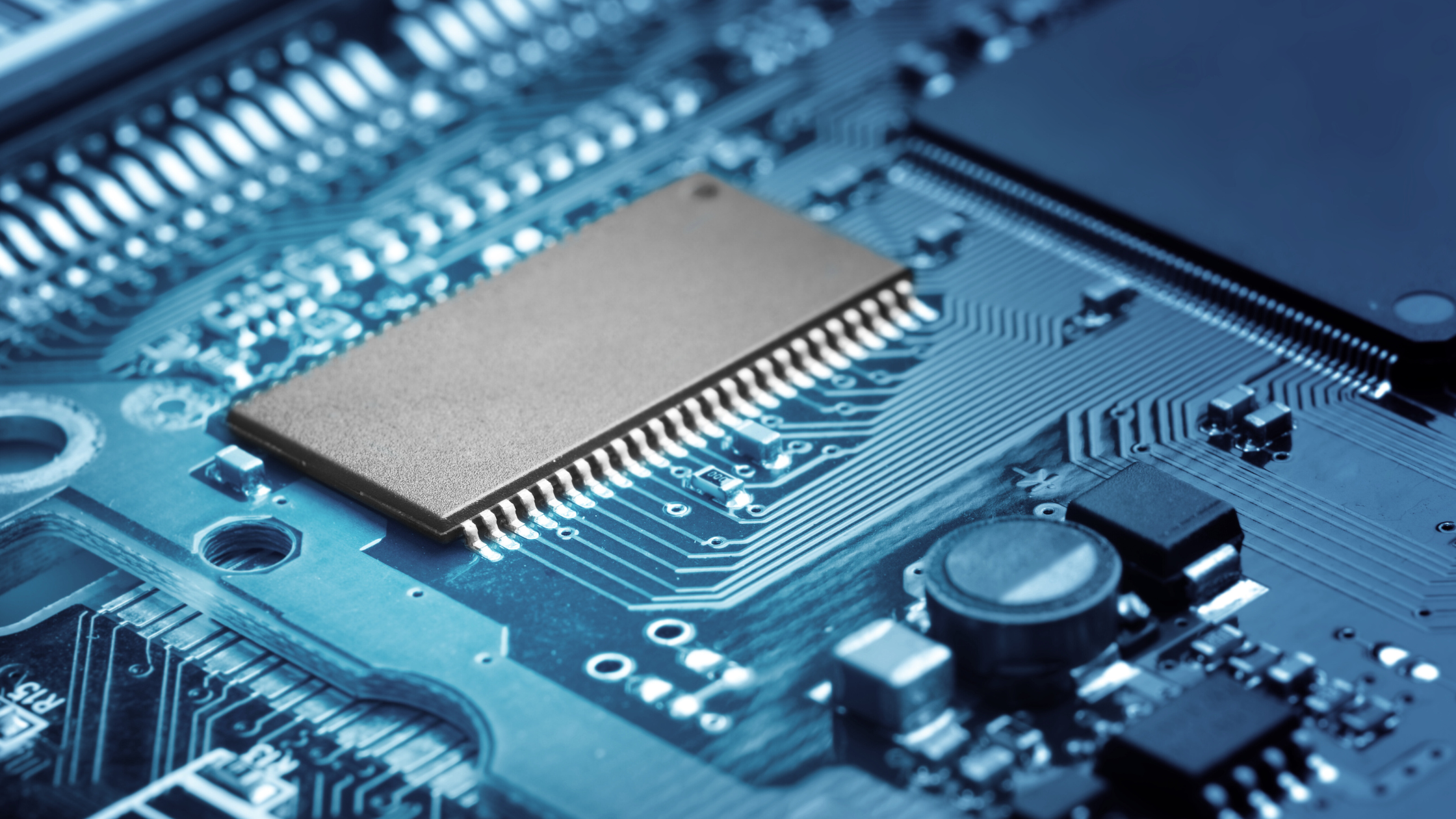
At its core, the Blackwell B200 is not a single piece of silicon. It represents a masterclass in semiconductor technology through its multi-die design. It features 208 billion transistors across two closely coupled dies, manufactured using a custom 4NP TSMC process.
What makes this a breakthrough is the high speed interconnect a 10 TB/s chip to chip link that allows these two dies to function as a single, unified processor. This solves the “reticle limit” problem, where the physical size of a single chip is limited by the machinery used to etch it. By seamlessly bonding two dies, this advanced hardware overcomes physical manufacturing constraints while maintaining the low latency required for complex AI workloads.
Why This Hardware Breakthrough Matters Now
The timing of this innovation is critical. Large Language Models (LLMs) are now crossing the threshold of trillions of parameters. Previous generations of AI hardware were struggling with “memory wall” issues where the processor spends more time waiting for data than actually computing.
By integrating 192GB of high bandwidth memory (HBM3e), Blackwell provides the massive throughput necessary to keep the processing cores fed. This shift is essential for the next phase of “Agentic AI,” where models must process multimodal data (video, voice, and text) in real-time without the lag that characterizes current cloud-based systems.
Performance, Efficiency, and the Power Challenge
When compared to the previous H100 (Hopper) generation, the impact is staggering. Blackwell offers up to a 5x increase in AI inference performance. However, the most vital metric for the industry is energy efficiency. Next-generation computing is increasingly constrained by the power grid; Blackwell reduces LLM inference energy consumption and costs by up to 25 times compared to its predecessor.
This efficiency is achieved through a dedicated Transformer Engine that dynamically adjusts the precision of calculations. By using lower bit numerical formats (FP4 and FP6) where high precision isn’t necessary, the hardware can perform more work with significantly less electrical draw.
Implications for Cloud and Edge Computing
The arrival of such dense compute power is forcing a redesign of the modern data center. We are seeing a shift toward liquid cooling as a standard requirement, as these chips operate at power densities that traditional air cooling cannot manage.
While Blackwell targets the cloud, its architectural breakthroughs will inevitably trickle down to edge-AI hardware. The techniques used to manage power and memory in these massive chips provide the blueprint for more efficient, AI-capable chips in robotics and autonomous vehicles. As businesses look to integrate these capabilities, understanding the broader landscape of emerging technologies buyers cant ignore in 2025 becomes essential for strategic planning.
Market and Ecosystem Impact
The shift to Blackwell has sparked a massive CAPEX cycle among Hyperscalers like Microsoft, Amazon, and Google. For investors and startups, this hardware represents a “moat.” Enterprises that can secure access to this advanced hardware can train larger models faster and at a lower cost per token than those relying on legacy architecture.
Furthermore, this breakthrough has accelerated the custom silicon trend. Seeing the success of Blackwell’s multi-die approach, competitors and even cloud providers (via projects like AWS Trainium) are doubling down on chiplet-based designs to avoid being left behind in the emerging hardware trends of the decade.
Why this innovation matters for the future of technology
The Blackwell architecture marks the end of the “single-chip” era and the beginning of the “system as a chip” era. It proves that physical hardware constraints can be overcome through sophisticated packaging and high-speed interconnects rather than just shrinking transistors. This breakthrough ensures that AI development will not be throttled by hardware limitations for the next several years. Ultimately, it paves the way for more sustainable, energy-efficient data centers that can handle the massive computational weight of future artificial general intelligence.
Leave a Reply